| Layer Absorptance option allows you to represent a level of absorptance in individual layers of the design as a function of wavelength (Spectral mode) or angle of incidence (Angular mode).
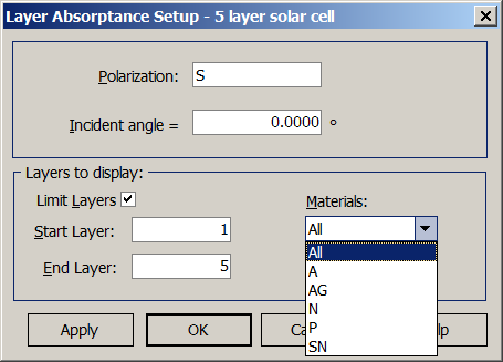
Layer Absorptance Setup dialog allows you to select Polarization state and Incident angle (or wavelength value in Angular mode) for this analysis. It is also possible to limit display to a range of layers (Start Layer and End Layer entries) and to just one of available set of Materials. Recently developed design option allows you to optimize absorptance in selected layers. See also our video example on YouTube |
 |
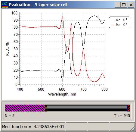
| Example: 5-layer design for thin film solar cell (M. Zeman, Optical modeling of a- Si:H solar cells with rough interfaces: Effect of back contact and interface roughness, J. of Appl. Phys., 2000, Vol. 88):
Ag – 300 nm n-a-Si – 20 nm i-a-Si – 600 nm p-a-Si – 9 nm SnO2 – 16 nm |
|
| It is possible to display Layer Absoptance at the Evaluation window together with other spectral characteristics.
|
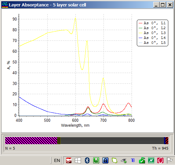
Layer Absoptance in separate layers can be plotted in a special Window: Analysis –> Layer Absorptance
|
OptiLayer provides user-friendly interface and a variety of examples allowing even a beginner to effectively start to design and characterize optical coatings. Read more…
Comprehensive manual in PDF format and e-mail support help you at each step of your work with OptiLayer.
If you are already an experienced user, OptiLayer gives your almost unlimited opportunities in solving all problems arising in design-production chain. Visit our publications page.
Look our video examples at YouTube
OptiLayer videos are available here:
Overview of Design/Analysis options of OptiLayer and overview of Characterization/Reverse Engineering options.
The videos were presented at the joint Agilent/OptiLayer webinar.