| Trapping option can be used for solving some sophisticated design problems.
The Trapping option can be used for preventing grows of thicknesses of some layers, for example, thicknesses of metal layers above a reasonable threshold level. This option can be also used for suppressing development of thin design layers in the course of design procedure. It is especially useful for EUV and X-Ray applications. If Trapping is active, then in the course of coating designing with the help of various OptiLayer design options specified trapping limits are included in the design procedure. This means that thickness of any design layer once getting inside specified limits will stay inside these limits. |
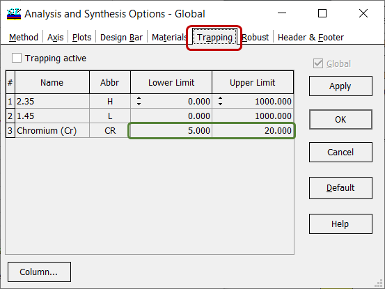
Trapping option can be activated through Synthesis –> Options –> Trapping tab in Analysis and Synthesis Options
Fig. 1. Trapping tab: settings of allowed limits of layer thicknesses. |
| Design example: A beamsplitter should reflect more than 50% from its front side and almost zero from its back side. The optical element should operate in the visible spectral range 380-780 nm and in the angular range from 0 to 45°, average polarization. Such a beamsplitter can be used, for example, for sun glasses.
According to the thin-film theory, such a beamsplitter must comprise metal layers in order to obtain reflectance different from the front and back sides of the optical element. For example, as a metal, Cr might be used. Imagine, that because of some technological limitations the thicknesses of Cr layers should be between 5 and 20 nm. First, we can try with the standard needle optimization (Fig. 3). The obtained designs will comprise thick Cr layer (for example, 100 nm as in the solution shown in Fig. 2). |
|
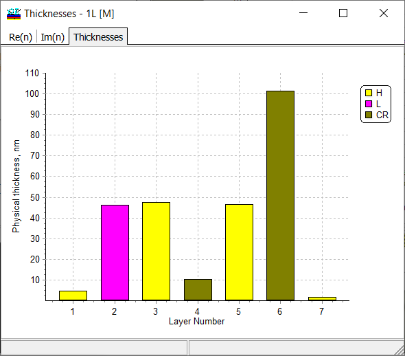
Fig. 2. Refractive index profile of a 8-layer solution obtained without trapping. The last Cr layer (layer number 6) is much thicker than 20 nm. |
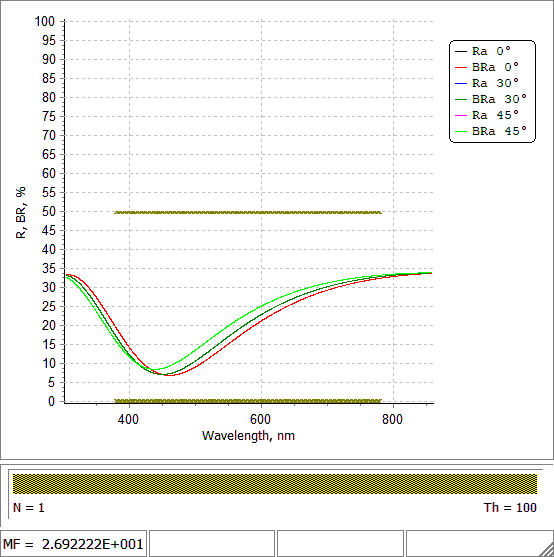
Fig. 3. Design without trapping option (needle optimization in automatic mode). |
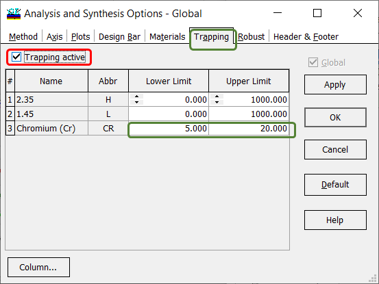
Fig. 4. Activation of trapping option. |
If we activate the Trapping option (lower and upper limits for Cr layers are 5 and 20 nm, Fig. 4) and apply a standard algorithm again (Fig. 6), we obtain solutions with Cr layers not thicker than 20 nm (for instance, a design shown in Fig. 5).
Actually, spectral performance of designs obtained with active Trapping option can be worse than performance of the designs without trapping. The feasibility demand is, however, fulfilled. Of course, Trapping is one of a large variety of design techniques of OptiLayer. It can happen that other techniques will provide better results. It should be noted as well that in the course of the needle optimization, a very thin layer of a “trapping material “can be inserted between other two layers of the “trapping material”. In this case, all three layers will be merged and the upper limit will be violated. It means that your problem does not benefit from the harnessing of the Trapping option. |
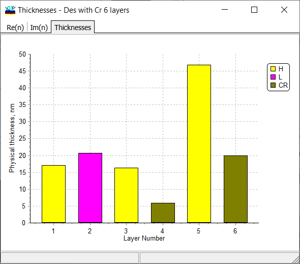
Fig. 5. Refractive index profile of a 6-layer solution obtained with active trapping. Both Cr layers are thinner than 20 nm. |

Fig. 6. Design with trapping option (needle optimization in automatic mode). |
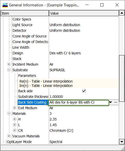
Fig. 7. In order to reduce the back side reflectance, an 6-layer anti-reflection coating is added on the back side. It can be done through the General Information window. |
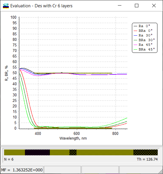
Fig. 8. Reflectance and back side reflectance of the designed optical element (beamsplitter). |
OptiLayer provides user-friendly interface and a variety of examples allowing even a beginner to effectively start to design and characterize optical coatings. Read more…
Comprehensive manual in PDF format and e-mail support help you at each step of your work with OptiLayer.
If you are already an experienced user, OptiLayer gives your almost unlimited opportunities in solving all problems arising in design-production chain. Visit our publications page.
Look our video examples at YouTube
OptiLayer videos are available here:
Overview of Design/Analysis options of OptiLayer and overview of Characterization/Reverse Engineering options.
The videos were presented at the joint Agilent/OptiLayer webinar.