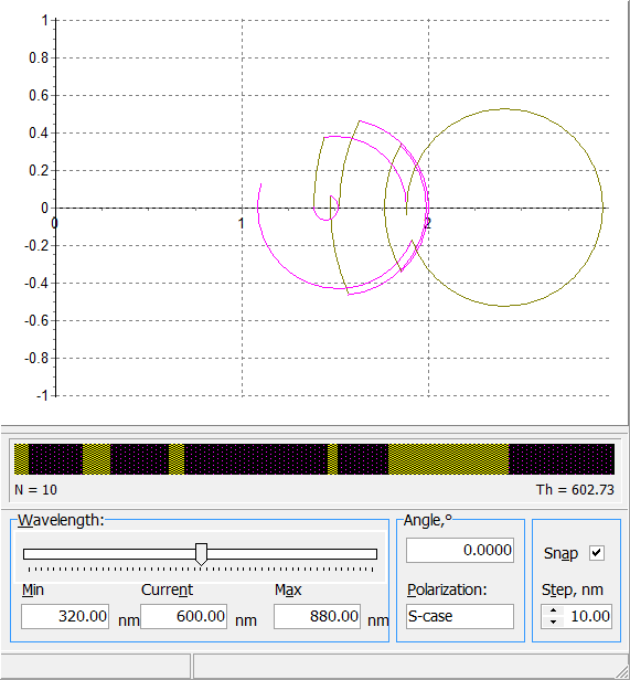
| OptiLayer shows you an Admittance diagram for the current design. The design is represented by the design bar showing layers in different colors, the number of layers N and the overall physical thickness Th.
You can select the wavelength value at which you want to see the admittance plot by moving the slider in the Wavelength window. The overall spectral range for the slider is shown (and can be modified) in the Min and Max edit boxes; the current position of the slider is shown by the wavelength value in the Current field. You can stop the slider at certain positions if you check the box Snap in the lower right corner of the window. The slider can stop only at positions defined by the minimum wavelength value and the increment defined in the Step edit field. Note that the increment is always set in nanometers, and must be in the range from 1 to 100. You can also set the Angle of incidence and Polarization state (S, P or Both) in the corresponding edit boxes. Angular and Spectral Modes also can be switched in the Admittance window with right-click popup menu. In the Angular mode Admittance window will allow you to study angular dependence of admittance diagram.
|
Example: Admittance diagram of a 10-layer anti-reflection design for different wavelengths (put mouse button on the picture).
|
OptiLayer provides user-friendly interface and a variety of examples allowing even a beginner to effectively start to design and characterize optical coatings. Read more…
Comprehensive manual in PDF format and e-mail support help you at each step of your work with OptiLayer.
If you are already an experienced user, OptiLayer gives your almost unlimited opportunities in solving all problems arising in design-production chain. Visit our publications page.
Look our video examples at YouTube
OptiLayer videos are available here:
Overview of Design/Analysis options of OptiLayer and overview of Characterization/Reverse Engineering options.
The videos were presented at the joint Agilent/OptiLayer webinar.