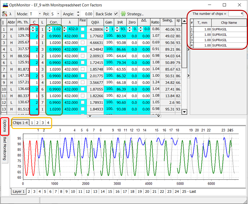
| In the case, if you use the indirect monochromatic monitoring (i.e. monitoring with witness chips, OptiLayer suggests you tools for generating the corresponding monitoring spreadsheet and monochromatic monitoring simulation (Fig. 1).
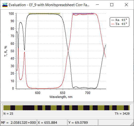
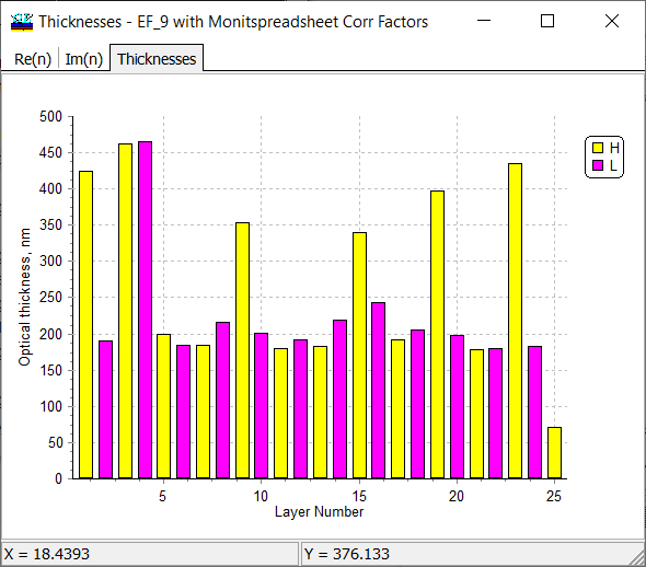
It is better to demonstrate the powerful indirect monitoring option using an example. Example: a 25-layer edge filter operating at the angle of incidence of 45 degrees and exhibiting high reflectance in the range 583-683 nm and high transmittance in the range 670-710 nm. Spectral reflectance and transmittance of the filter are shown in Fig. 2 and its refractive index profile is shown in Fig. 3. The design comprises layers of high-index material Nb2O5 with n=2.2 and low-index material SiO2 with n=1.47. Materials abbreviations are H and L, respectively.
|
Fig. 1. Monochromatic monitoring simulation of the 25-layer edge filter. Four witness chips are involved (see on the top of the window). |

Fig. 2. Oblique incidence reflectance and transmittance of the 25-layer edge filter. |

Fig. 3. Refractive index profile of the 25-layer edge filter. |
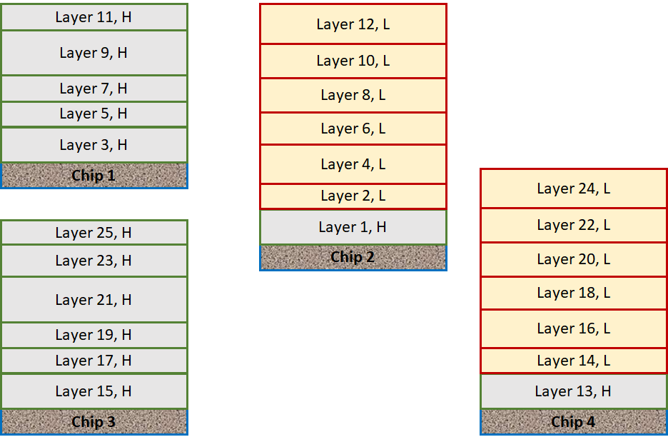
| In order to monitor the deposition of the edge filter, four witness chips were chosen. The distribution of design layers is shown in Fig. 4. Chips 1 and 3 contain H-layer only. The first layers on Chips 1 and 3 are H-layers and the next layers are L-layers. | |

Fig. 4. Layer distribution on four chips. Actually, at the end of the deposition, chips 1 and 3 will consist of only one thick H-layer. |
|
| In the Monitoring spreadsheet (Results –> Monitor), the layer distribution on chips should be specified in column C (Chip). The number of chips and the substrates should be specified on the right-side panel. Also, it may be known that due to technological reasons, the thicknesses of layers on the sample substrate and the thicknesses of layers on the chips can be different. In order to take these differences into account, correction factors can be specified (column Corr.) In our example, we assume that all H-layers are over-deposited by 2% and all L-layers are under-deposited by -1% (see 1.02 and 0.99 corrections in Corr. column). | |

Fig. 5. Monitoring spreadsheet generated for 4 chips (Suprasil), distribution of layers is schematically shown in Fig. 4. On the bottom panel, you can switch between all separate layers (with Chips 1-4 tab) or separate layers corresponding to separate chips (1, 2, 3, and 4 tabs). Using Options button, you can specify some important settings (see Fig. 6). |
|
| Important: to be able to specify chips and related issues, you need to check Permit reusing Chips check box. | |
|
Fig. 6. In order to be able to specify witness chips, Permit reusing chips check box must be checked: Options (left Options tab) –> Options button –> Misc. tab in Monitoring Spreadsheet Options window. |
|
|
Fig. 7. Column L in the Monitoring spreadsheet indicates the number of the layer on the current witness chip. Design layers 15, 17, 19, 21, 23, and 25 correspond to layers 1-6 on the witness chip 3 (see positions in L-column outlined by blue). Bad Monitoring tab (left vertical panel) can be pin to the window. |
|
|
Fig. 8. Monochromatic monitoring simulation of the 25-layer edge filter design shown in Fig. 3 assuming monitoring spreadsheet from Fig. 5 and settings mentioned here. |
Fig. 9. Resulting performance of one of the simulated deposition runs. |
Look our video examples at YouTube
OptiLayer videos are available here:
Overview of Design/Analysis options of OptiLayer and overview of Characterization/Reverse Engineering options.
The videos were presented at the joint Agilent/OptiLayer webinar.