| OptiLayer provides Error Analysis and Error Yield Analysis of stacks, i.e. a set of thick media with optional coatings at each boundary between them.
Disturbed designs are calculated in the similar way as in the case of statistical errors analysis of conventional coatings. Error analysis and Error Yield Analysis are powerful OptiLayer tools to study stability of design solutions to inevitable deposition errors. Due to its high computational power, OptiLayer allows you to perform many hundreds and thousand statistical tests very fast. |
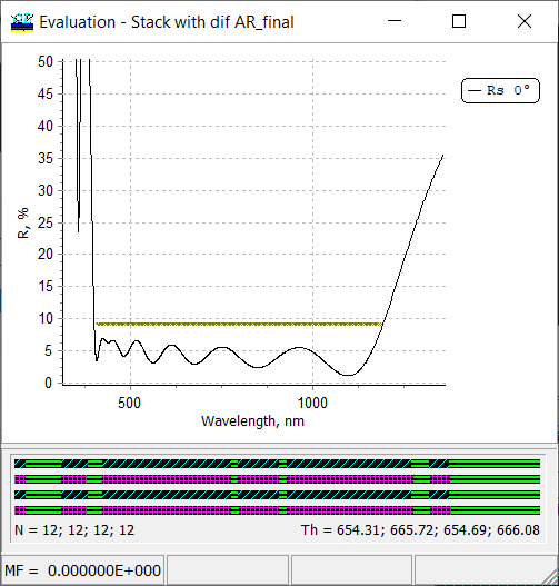
Fig. 1. Spectral characteristic of a stack containing four AR coatings. The stack operates in the range from 400 to 1200 nm. Error bars on the bottom panel represent designs in the stack. Thin-film materials are Nb2O5, TiO2, and SiO2. |
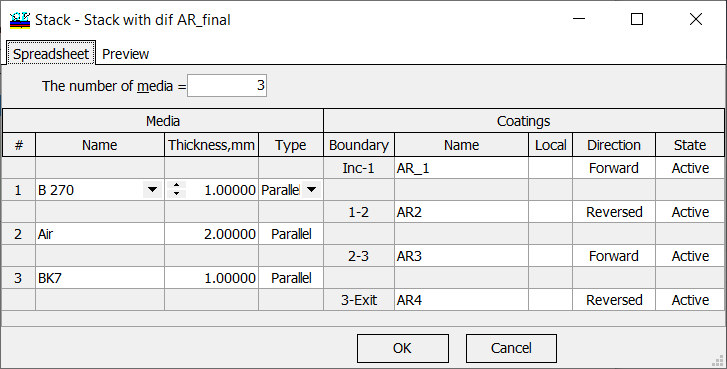
Fig. 2. Example. A stack consists of two substrates (B270 and BK7) separated by an air gap. Each surface is coated by AR coatings. |
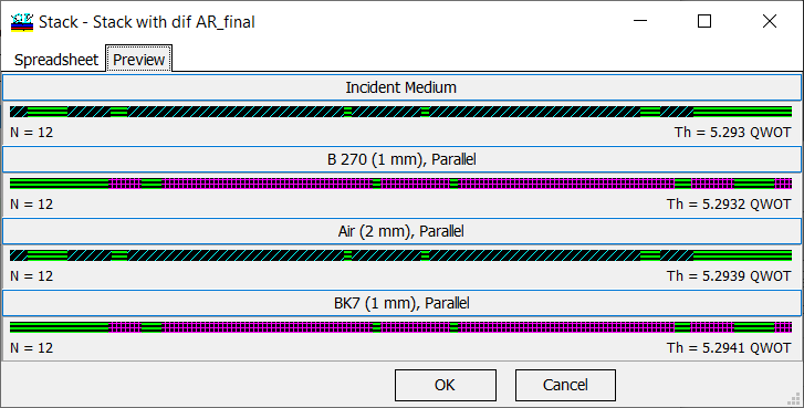
Fig. 3. The stack from Fig. 2 represented AR coatings in a graphical form. |
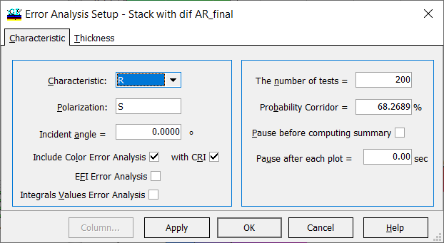
Fig. 4. Settings for error analysis in stacks. Color Error Analysis and CRI are also involved. |
In order to perform statistical error analysis, you should specify the corresponding parameters in Error Analysis Setup window: a spectral characteristic, polarization, incident angle, optionally color error analysis and CRI, or integral values (Fig. 4, left panel). On the right panel, you should specify the number of statistical tests (disturbed designs), and probability corridor.
Levels of thickness errors are specified on the Thickness tab. |
| Thickness tab of Error Analysis Setup is subdivided into three sub-tabs, each of them allows you to specify errors in layer thicknesses. The settings are the same as in the case of the statistical error analysis of conventional coatings.
In Coating sub-tab (Fig. 5), it is possible to specify absolute or relative errors in all layers of each coatings of the stack. In Materials sub-tab (Fig. 6), you can specify errors in layers of thin-film materials. Error Analysis and Color Error Analysis are shown in Figs. 8, 9, 10, and 11. In Thickness sub-tab (Fig. 7), a fine tuning of deposition errors through the entire stack can be set up.
|
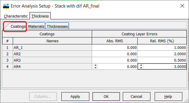
Fig. 5. Settings of errors in AR coatings. Level of relative errors are 1%, 2%, 0.5%, and 3%. |
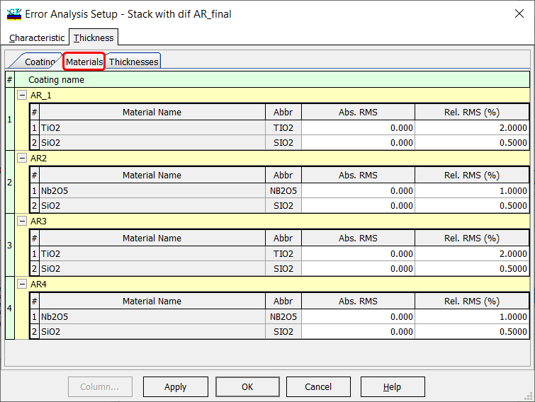
Fig. 6. Relative errors of 2%, 0.5%, and 1% are specified in TiO2, SiO2, and Nb2O5 layers. |
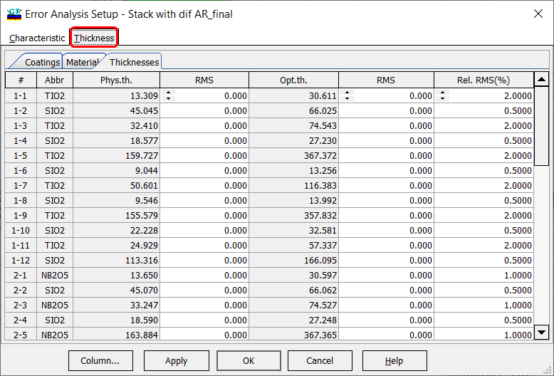
Fig. 7. Relative errors of 2%, 0.5%, and 1% are specified in TiO2, SiO2, and Nb2O5 layers. Using this Thickness sub-tab, you can specify error in each layer separately. This option is typically used for fine turning of expected errors. |
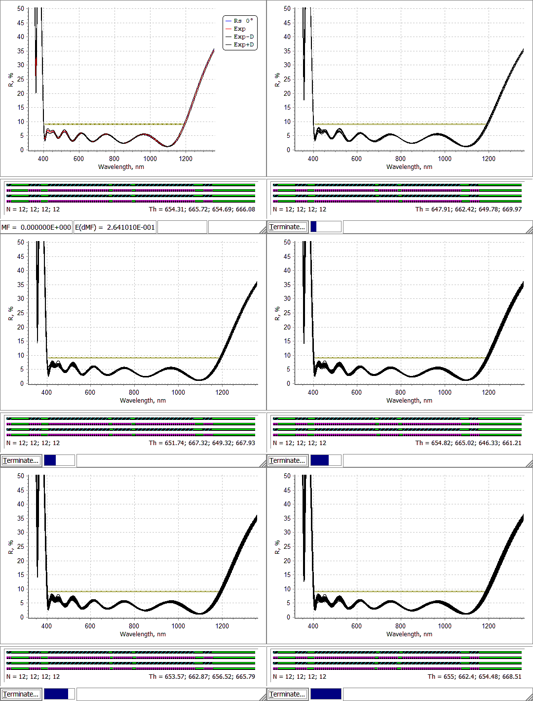
Fig. 8. Error analysis process for settings shown in Fig. 6. |
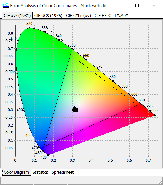
Fig. 9. Error analysis process for settings shown in Fig. 6. Error analysis of colors can be performed independently, i.e. it does not matter, whether a color target is specified. |
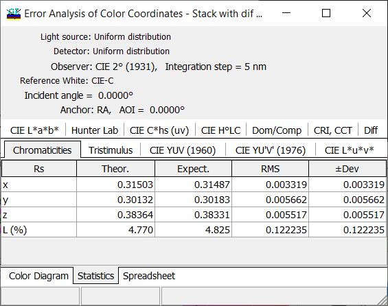
Fig. 10. Numerical values of the color deviations are presented in Statistics tab of the Error Analysis of Color Coordinates. Expect. denotes the average value of the color coordinates of disturbed designs and RMS and (\(\pm\) Dev) show root square deviation and deviations calculated for the specified value of Probability Corridor, respectively (Fig. 4). |
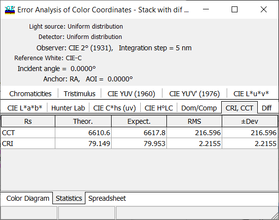
Fig. 11. Numerical values of CRI deviations are presented in Statistics tab of the Error Analysis of Color Coordinates. Expect. denotes the average value of CRI of disturbed designs and RMS and (\(\pm\) Dev) show root square deviation and deviations calculated for the specified value of Probability Corridor, respectively (Fig. 4). |
| In Error Analysis of Integrals, Values, theoretical integral values and their deviations are represented. Here you can see averaged expected values (Expect.), root mean square deviations (RMS), and deviations calculated for Probability Corridor (\(\pm\) Div) (Fig. 4).
OptiLayer calculates statistical expectations and deviations of all values specified in Integrals, Values window. It does not matter whether these values in integral target indicated. The Error Analysis of Integral, Values window has the same fonts, colors as Integral, Values window. Starting from the most recent version 12.83, you can define your own formatting style and restore it in all other problem directories. |
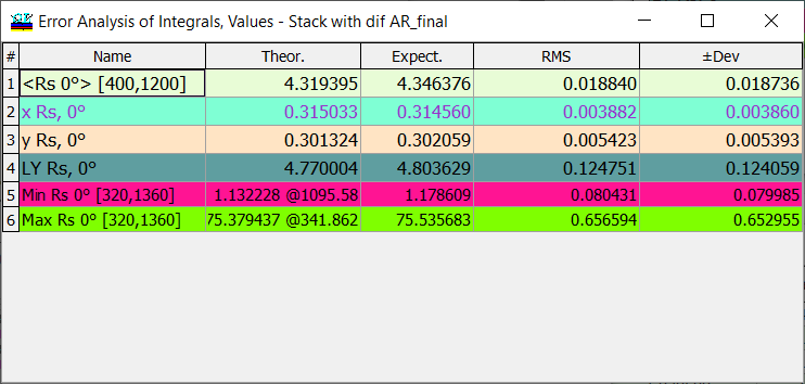
Fig. 12. Numerical values of deviations Integral values presented in Error Analysis of Integrals, Values. Expect. denotes the average value of the color coordinates of disturbed designs and RMS and (\(\pm\) Dev) show root square deviation and deviations calculated for the specified value of Probability Corridor, respectively. |
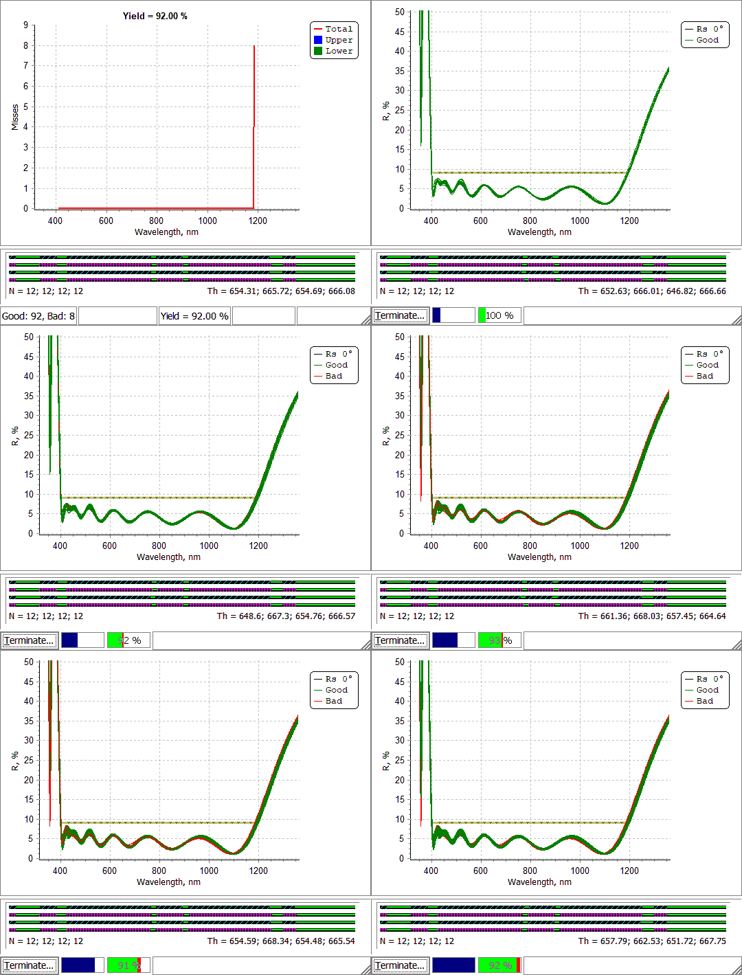
Fig. 13. Error Yield Analysis of the stack (Figs. 1 and 2) with settings shown in Figs. 6 and 7. |
OptiLayer allows you to estimate production yield of stacks in the same way as production yield of conventional coatings. Errors in layer thicknesses are specified using Thickness tab of the Error Analysis Setup window (Figs. ).
Yield bar on the bottom of the yield analysis window shows the current yield value. The number of statistical tests should be not very large in order not to slow down the calculations and not low in order to have a representative set of disturbed designs. More details can be found here. |
| If spectral characteristics for multiple incidence angles and polarization are plotted in Evaluation window, then in the case of Error Yield Analysis, spectral characteristics of the disturbed designs are shown for all these angles and polarization states.
At the same time, yield estimations are performed only for AOI/polarization specified in the loaded range target. Example in Fig.14: range target is specified for normal incidence, reflectance curves for 30 and 45 degrees, averaged polarization are shown as well.
|
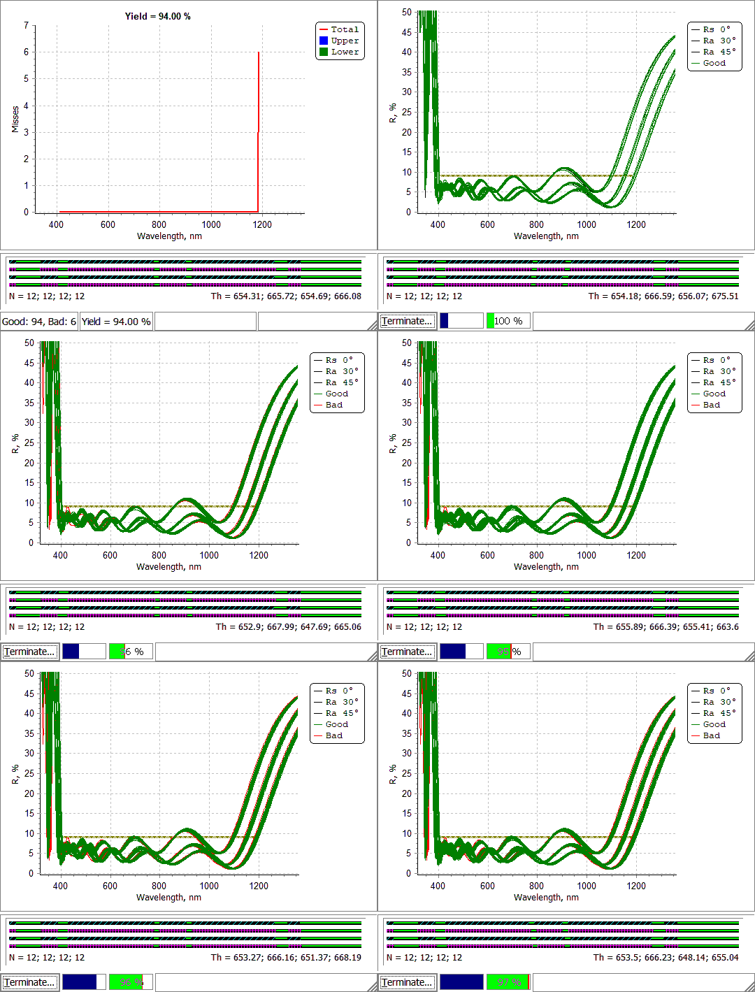
Fig. 14. Error Yield Analysis of the stack (Figs. 1 and 2) with settings shown in Figs. 6 and 7. Yield is calculated for normal incidence, other two curves provide an impression of behavior of the disturbed spectral curves at oblique incidence. |
Look our video examples at YouTube
OptiLayer videos are available here:
Overview of Design/Analysis options of OptiLayer and overview of Characterization/Reverse Engineering options.
The videos were presented at the joint Agilent/OptiLayer webinar.