|
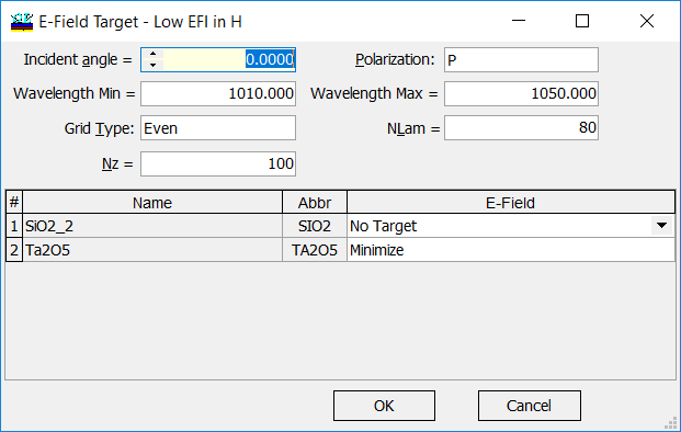
Electric Field Target allows to Minimize or to Maximize a squared modulus of the electric field amplitude \(|E|^2\). Electric filed editor allows to specify
Example: It was demonstrated that by suppressing the electric field in high-index layers and shifting its maxima to low-index layers the damage threshold can be increased by 30%. The design of the coating with optimized electric field intensity (EFI). The laser central wavelength was 1030nm, the high reflectance range is from 960 to 1100 nm. Thin film materials are Ta2O5 and SiO2, substrate is Fused Silica.
|
The target was a combination of two targets: (1) conventional one with target reflectance of 100% in the range from 960 to 1100 nm and (2) electric-field intensity target with minimized intensity in Ta2O5 layers (see above). |
Refractive index profile of a 35-layer Quarter-Wave Mirror, thin film materials are Ta2O5/SiO2: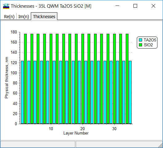 |
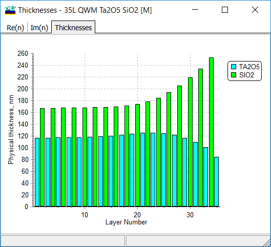
Refractive index profile of the optimized design with
reduced electric field intensity (EFI) inside the Ta2O5 layers:
 |
|
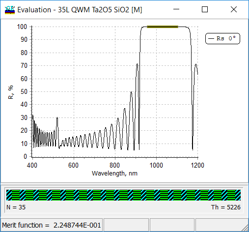
Reflectance of the 35-layer Quarter-Wave Mirror:
|
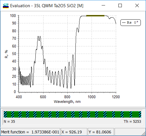
Reflectance of the design with optimized electric-field intensity:
|
|
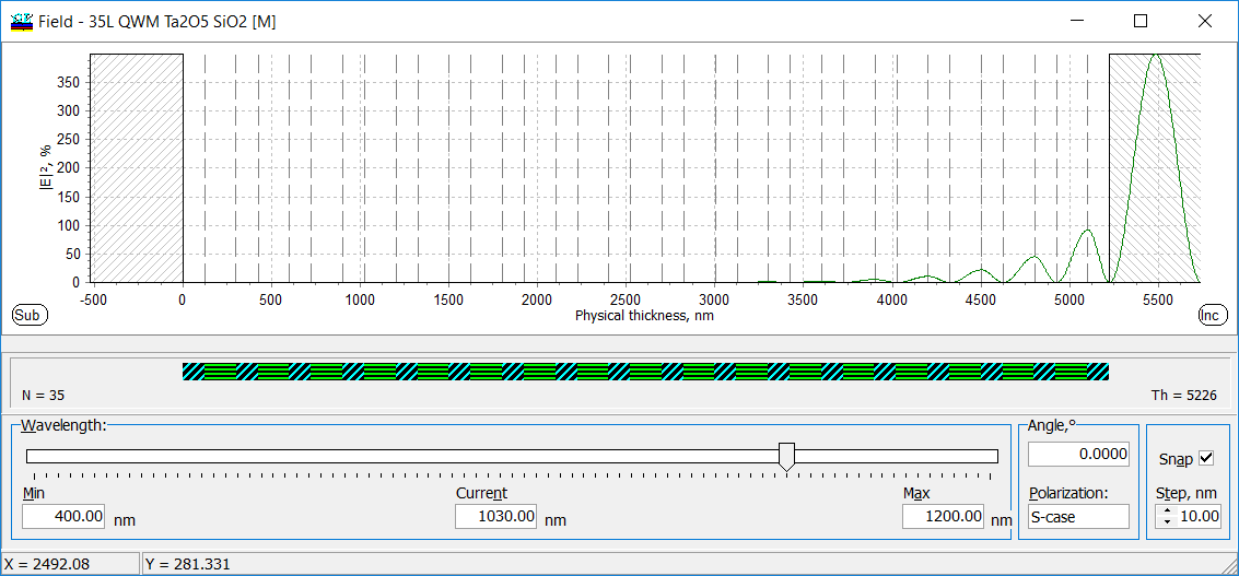
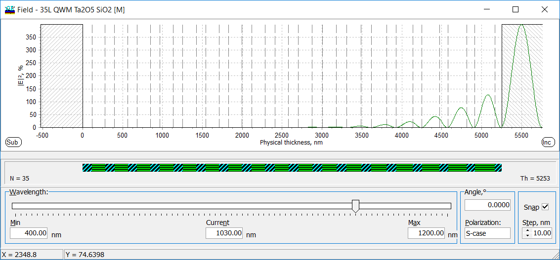
Electric field distribution in the 35-layer quarter-wave stack:
|
Electric field in Ta2O5 layers is reduced:
|
OptiLayer provides user-friendly interface and a variety of examples allowing even a beginner to effectively start to design and characterize optical coatings. Read more…
Comprehensive manual in PDF format and e-mail support help you at each step of your work with OptiLayer.
If you are already an experienced user, OptiLayer gives your almost unlimited opportunities in solving all problems arising in design-production chain. Visit our publications page.
Look our video examples at YouTube
OptiLayer videos are available here:
Overview of Design/Analysis options of OptiLayer and overview of Characterization/Reverse Engineering options.
The videos were presented at the joint Agilent/OptiLayer webinar.

